Dumping the Super Game Boy 2 boot ROM
I'm happy to announce that I've succeeded in dumping the Super Game Boy 2 boot ROM. I take my hat off to Costis Sideris, who managed to dump the original Super Game Boy boot ROM, and documented the procedure with enough details for other people to follow his footsteps. I basically just replicated the same steps on the SGB2 with slightly different tools. The entire process took all my free time on three evenings, but it was fun and we finally have a verified dump of the SGB2 boot ROM! While doing hardware research for my Mooneye GB emulator, I've acquired a lot of hardware that made it possible to do this. Unlike in the original SGB hack, no FPGA was used.
Skip to the end if you just care about the result
How was it done?
From a high-level perspective, we basically just want to prevent the boot ROM from hiding itself. One of the last instructions in the boot ROM writes to the register $FF50, which hides the boot ROM permanently. There is no way to execute custom code before this, so we need to completely prevent the instruction from executing. There are a few things that are needed:
- The CPU clock needs to be controlled
- We need the ability to raise the clock to 24 MHz to overclock the CPU. Overclocking confuses the CPU, so it goes crazy and hopefully will not execute the instruction that hides the boot ROM
- There needs to be a trigger that can turn overclocking on at the right time
- Once we get past the boot ROM to cartridge space, we need a program that dumps the low 256 bytes containing the boot ROM
Controlling the CPU clock
The first step was to find out how the CPU clock is generated and how it could be substituted with an external clock. The CPU in SGB2 uses the same amount of pins as SGB but a different pinout. Therefore, even though there are schematics for SGB, I had to trace some signals to understand the clock generation in detail. In the end I decided to trace all signals on the board, and I plan to publish an interactive PCB visualization of the SGB2 in a later blog post. But for the purposes of this blog post, it's enough to know that CPU pin 67 is connected to ICD2 pin 3, which has the CPU clock signal.
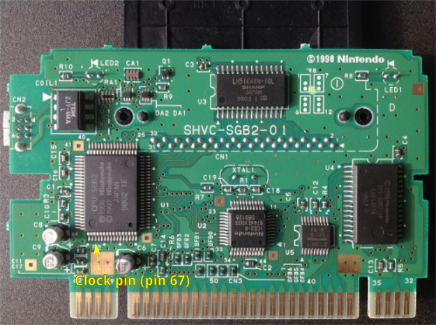
The SGB uses a divided clock signal from the SNES/SFC, while the SGB2 uses a separate clock crystal. Therefore an SGB is always slightly off from the normal Game Boy frequency (4.194304MHz), while an SGB2 is not. In both cases the ICD2 chip handles the low-level clock generation, and the CPU simply gets the clock using one pin from the ICD.
My solution was to very surgically lift the clock pin of the CPU without causing any other permanent damage. I did not want to take out the crystal, because it's part of a small circuit and as far as I know could not be directly replaced with a clock signal. One option would've been to lift two ICD2 clock pins, but I decided that one CPU pin would be easier and less risky. I managed to lift the clock pin (pin 67), and soldered a simple connector to make it easy to plug different clock sources. This would later enable me to also connect it back to the ICD2 to restore normal behaviour.
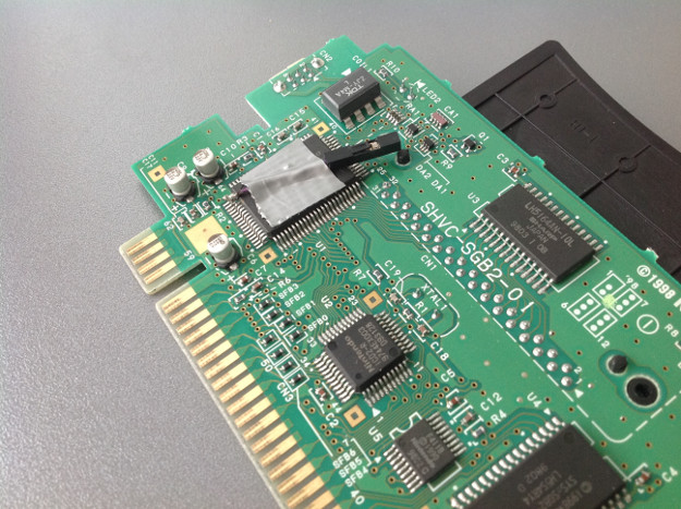
Lifted pin + connector
First experiments with an Arduino
I wanted to quickly test if controlling the clock would even work on SGB2, and whether the SGB2 survived the soldering or not. I have an Arduino Uno device I normally use for peeking and poking Game Boy cartridges. It's quite simple to make the Arduino output a 50% duty cycle PWM signal, but the small CPU frequency (16 MHz) limits the possible output frequencies, so the Arduino would not suffice for overclocking in the final dumping procedure. I wrote a simple Arduino program that set up a 2 MHz PWM signal, and connected everything. The Arduino uses 5 V levels, so it was directly compatible with the SGB2.
After connecting everything, I started the Arduino and the SGB2, and was greeted by SGB2 and Nintendo logos, and a half-speed Tetris! So, even an Arduino could be used as a clock for the SGB2. However, I needed something a bit more powerful to reach that 24MHz frequency needed for the overclock.
Triggering the overclocking
Generating a clock signal was a nice milestone, but I still needed to implement the higher frequency signal and a trigger for it. The original solution used the FPGA to listen to the address bus, and counted cycles to know exactly when to start overclocking the CPU. Since I wasn't using an FPGA, I needed some clever way to implement the triggering.
Earlier this year I designed breakout boards for Game Boy cartridges so I could use my Open Bench Logic Sniffer to do logic analysis on the cartridge bus. The logic sniffer has a TRGO pin that is connected directly to the FPGA chip. I realized that I could connect it to a microcontroller and use an interrupt to trigger the overclocking. Interrupt handling has a significant delay, so the overclocking would not be triggered immediately, but by nudging timings back and forth I could align the overclocking where I wanted it.
Boot ROM opcode fetches are not visible in the cartridge bus, but IO register and cartridge accesses are. At first I triggered sniffing when the $FF50 register was written to, but this would be too late to start overclocking, especially considering the interrupt handling delay. However, a couple of instructions before writing to $FF50, the boot ROM accesses $FF13 and $FF14, and I was able to set up a chained trigger that would trigger the logic analyser on the $FF14 access. This would also be visible in the TRGO pin and could be used to start the overclocking in the microcontroller.
Teensy to the rescue!
In addition to the Arduino, I also have a Teensy 3.1 microcontroller. It's based on a ARM Cortex-M4 core, which is significantly more powerful than the simple Atmel in the Arduino. I ran the Teensy in 96 MHz mode, which made it very straightforward to set up 2 MHz and 24 MHz signals. The basic idea is still the same: set up 50% duty cycle PWM and set up an interrupt handler that temporarily raises the frequency. Teensy uses 3.3 V logic, but is 5 V tolerant in most pins. Initially I was preparing to use an Adafruit #395 level converter, but a quick test confirmed that 3.3 V clock signal was enough for the SGB2.
Here's the Teensyduino program I ended up using:
const int TRIGGER_PIN = 2;
const int CLKOUT_PIN = 6;
const int BASE_HZ  =  2000000;
const int TURBO_HZ = 24000000;

void setup() {
  pinMode(TRIGGER_PIN, INPUT);
  pinMode(CLKOUT_PIN, OUTPUT);
  analogWriteResolution(2);
  analogWriteFrequency(CLKOUT_PIN, BASE_HZ);
  analogWrite(CLKOUT_PIN, 2);
  attachInterrupt(digitalPinToInterrupt(TRIGGER_PIN), intr, CHANGE);
}

#define NOP __asm__ __volatile__ ("nop\n\t")

void intr() {
  NOP; NOP; NOP; NOP; NOP;
  analogWriteFrequency(CLKOUT_PIN, TURBO_HZ);
  analogWrite(CLKOUT_PIN, 2);
  analogWriteFrequency(CLKOUT_PIN, BASE_HZ);
  analogWrite(CLKOUT_PIN, 2);
}

void loop() {
}
The program is fairly straightforward: we set up PWM with a specific frequency and wait for an interrupt. In the interrupt routine we do a few nops to nudge the timing a bit, then quickly switch to a turbo frequency and then back. The amount of nops was something I had to test with trial and error, and 5 nops is the final amount that made the entire procedure work.
The dumper program
Once the CPU skips the $FF50 register write, we need some kind of dumper program in the cartridge address space that can perform the actual dumping. The GB-BRK-M/F boards made it possible for me to use my EMS 64M flash cart for this purpose. Since the triggering was already done using a logic analyser, the cartridge itself doesn't need to do anything special. It just needs to be there when the CPU recovers from the overclocking and continues executing code.
I wrote a small dumper program that simply copies the first 256 bytes of the address space to the cartridge RAM. The dumper program also shows a small amount of bytes on the screen, so it was easy to visually verify whether the hack worked or not. A huge amount of nops was included in the beginning of the program, because the overclocking can cause the PC value to be pretty much anything. Adding $1000 nops means that basically any PC value under $1000 would lead the CPU to eventually execute the actual program.
Here's the code in wla-dx format. It uses an external common.s file from my Mooneye GB emulator repository.
.define CART_TYPE 3 ; MBC1+RAM+BATTERY
.define CART_ROM_BANKS 4
.define CART_RAM_SIZE 1

.incdir "../common"
.include "common.s"

  ; If the PC gets messed up, lots of NOPs makes it more probable that
  ; the CPU might still manage to take us to the following code
  nops $1000

  ; Set stack pointer just in case overclocking the CPU messed
  ; it up somehow. We are going to call memcpy so the stack has to work
  ld sp, $FFFE

  ; Enable cartridge RAM
  ld a, $0A
  ld ($0000), a

  ; Copy first 256 bytes to cartridge RAM
  ld hl, $A000
  ld bc, $100
  ld de, $0000
  call memcpy

  ; Disable cartridge RAM
  xor a
  ld ($0000), a

  ; Memory dump of first couple of bytes makes it quick to check
  ; if $FF50 failed or not
  ld hl, $0000
  ld a, $40
  jp dump_mem

; Recognizable pattern
.org $0000
  .repeat $50
    .db $42, $24
  .endr
Final setup
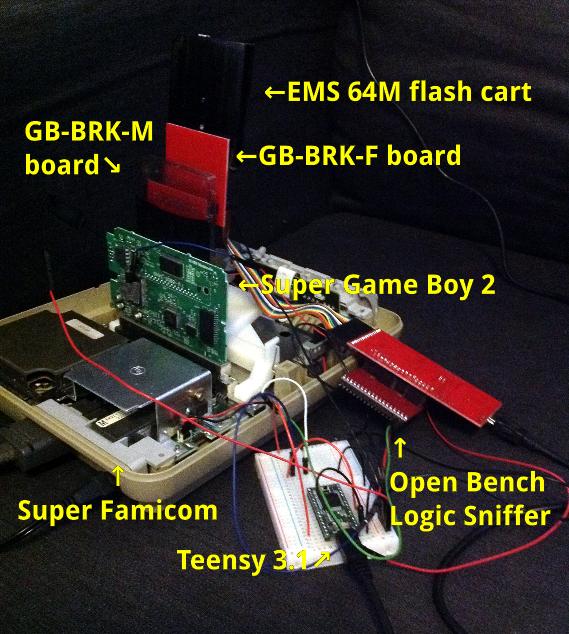
The final setup is a tall stack of devices and a mess of wires. Beautiful!
Performing the dump
The dumping required many attempts because there were multiple issues:
- There were random $FF13 and $FF14 addresses visible in the bus, which sometimes caused the logic analyser to trigger early
- The interrupt on Teensy did not always trigger correctly
- Sometimes the CPU stopped completely after the overclocking
- Sometimes the CPU ended up having a crazy PC value (e.g. $BCC0) after the overclocking
- Sometimes the CPU still executed the $FF50 write successfully
- Sometimes the SGB2 stopped working until the SNES was power cycled
- Sometimes the EMS cartridge stopped working until the SNES was power cycled
Some issues with the CPU behaviour were random, while some of them were dependent on exact timing. By adding some nops to the Teensy interrupt code I was able to slightly nudge the timing, which in the end gave me the result I wanted: the CPU failed to execute the $FF50 write and ended up having a PC register value in a sane range. The CPU then executed all the nops and ended up in the dumper program. Afterwards I just dumped the cartridge RAM using a USB cable and the ems-flasher tool. Success!
Here's some logic analyser pictures (click to enlarge). The zoom levels and positions are a bit different, so they are not directly comparable (sorry!).

Normal behaviour

Overclocked behaviour
Let's take a closer look at some important moments in the pictures!
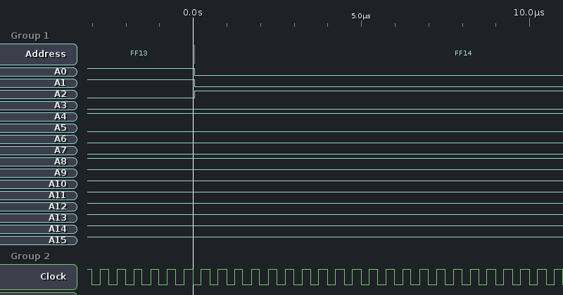
Trigger point (time 0.0s) is exactly at the $FF14 access. We can still see the $FF13 address latched in the bus even though the access happened much earlier.
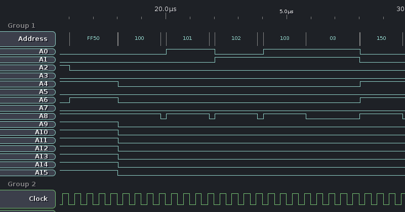
This is what the normal behaviour looks like. We can see the $FF50 access, and then the CPU starts fetching and executing code from $0100, $0101, $0102, etc.
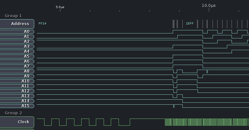
This is the overclocked behaviour. We see that the clock stops for a moment, while Teensy is reconfiguring the pin. Then we see the CPU going crazy once the overclocked signal appears.
At this zoom level we can't see all the addresses, but I took a closer look in the logic analyser software and $FF50 is not there!
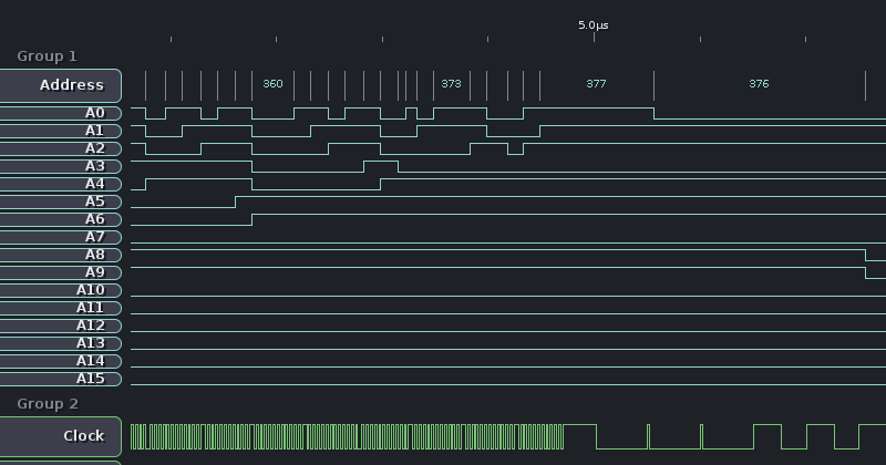
Here we can see the CPU still going crazy and accessing silly addresses. It even reads backwards ($0377, then $0376)! However, once the clock stabilizes, it continues execution from $0377 normally (unfortunately not visible in the picture).
Cool! So where can I get the ROM?
The ROM itself is probably the most anticlimatic and boring part of the entire thing. The SGB2 ROM differs from the SGB ROM by one byte. It's exactly the same difference as with DMG (Game Boy) vs MGB (Game Boy Pocket). I have no plans to host the ROM anywhere, so you can just create your own if you already have an SGB boot ROM.
The only difference is the byte at position $00FD. At that position SGB and DMG have the value $01, while MGB and SGB2 have the value $FF. This affects the value of register A that is written to the $FF50 register that hides the boot ROM. The register is never cleared, so the value is also visible to the actual program on the cartridge and can be used to differentiate between different hardware. In disassembled form the last two instructions are:
LD A, $FF          ; $00FC
LD ($FF00+$50), A  ; $00FE
                   ; $0100: cartridge ROM starts here
Here's some checksums of the SGB2 boot ROM for verification purposes:
- CRC32:
53d0dd63 - MD5:
e0430bca9925fb9882148fd2dc2418c1 - SHA-256:
fd243c4fb27008986316ce3df29e9cfbcdc0cd52704970555a8bb76edbec3988