Game Boy research status, March 2017
I've made some progress in my research, but don't have any mindblowing findings to share yet.
CPU versions
I've finally acquired all of the Game Boy CPU versions. CPU CGB A was the trickiest one, and the serial number of the unit doesn't make much sense when compared to data from my other units. So, unfortunately the data doesn't make it possible to predict which units would have that CPU version. The CPU CGB A unit doesn't work at the moment due to pretty bad battery leakage, but I'll attempt some repairs or even a CPU transplant if necessary. The board is CGB-CPU-01 and I've got several units with that board and CPU CGB and CPU CGB B.
I've also acquired a Game Boy Micro, but the CPU AGB E and the OXY-CPU-01 board are too small for any practical research with my tools. On the other hand, it doesn't really matter since OXY doesn't support pre-GBA games.
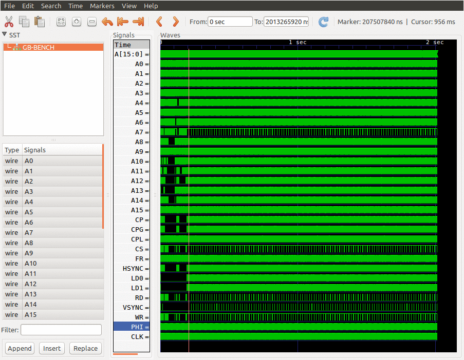
Game Boy reset, CLK vs PHI
On my SGB test bench, I found out that after RST is pulsed low, the Game Boy requires around 131072 clock cycles before the CPU wakes up and starts from $0000. The amount is not always the same, but clearly 2^17 = 131072 cycles is meaningful here. The first falling edge of CLK typically seemed to happen after 131076 T-cycles.
I also noticed that the CPU seems to have some activity four T-cycles before the first falling edge of CLK. At first this didn't make any sense, because I've always assumed the actual CPU machine cycles start with a rising edge on CLK because this always seemed to make sense based on the memory access timings and patterns. However, when cleaning up an AGB mainboard, I noticed the Ø (PHI) silk screen label on the pin I usually call CLK. I've seen it before, but this time something clicked in my head since I had read some 6502 CPU datasheets a while ago: what if the pin is not like the PHI0 or SYNC 6502 pin but more like the PHI1 pin. That is, what if it's a delayed or inverted version of the machine cycle clock, intended for external devices to let them know when they can do certain actions.
This realization calls into question my previous ideas about the CLK pin and the relative offset of timings.
Joypad interrupts
Joypad interrupts seem to be fully synchronous and don't trigger from a single falling edge or a quick low value on a P1 pin. It looks like there might be some hardware debouncing going on, because when a low value is sampled at a clock edge, the interrupt is triggered if and only if another low value is sampled a couple of clocks later. The intermediate values don't even seem to matter, so the interrupt triggers even if the pin is high for all the time except for two very specific clock edges. I can't remember the exact number of clocks, but roughly speaking something like this could trigger the interrupt:
4MHz clock: _|‾|_|‾|_|‾|_|‾|_|‾|_|‾|_|‾|_|‾|_|

1MHz clock: _|‾‾‾‾‾‾‾|_______|‾‾‾‾‾‾‾|_______|

Select btn: ‾‾‾‾‾‾‾‾|_|‾‾‾‾‾‾‾‾‾‾‾‾‾|_|‾‾‾‾‾‾‾
Moving the second low pulse even one clock edge earlier or later would not trigger the interrupt. And the signal could do anything between these two pulses and it would still trigger the same way. More research is needed...
Serial interrupts
Serial interrupts seem to be unrelated to the main clock when an external clock is select with the SC register. I did an experiment where I enabled serial interrupts, stopped the main clock completely, and pulsed the SCLK pin 8 times. The serial interrupt was triggered as soon as possible once the main clock was resumed. This seems to suggest the SCLK is directly connected to a shift register, and an internal flag is set after 8 bits have been shifted, regardless of what the main clock is doing.
I'll need to do more research, but if my findings are correct, I'll be able to trigger the internal serial interrupt flag at any time with one clock edge accuracy. This leads to several opportunities to have a better understanding of how HALT, STOP, and interrupts work.
Automated hardware testing
My work on automated testing has required a lot of time learning the world of FPGA/CPLD devices. My current focus is supporting these things in an automated way:
- hardware breakpoints
- clock edge counting
- full signal traces
Some things can already be done almost at full speed (in the MHz scale), but full signal traces are currently very slow (~1 KHz) which limits their usefulness.
I took a big signal trace of Tetris, starting from a hardware breakpoint at $0100 when the first instruction from the ROM is read. Here's a GIF in which I zoom the results in GTKWave until a single byte read from $0040 is visible: