Mooneye GB: Cartridge analysis - Wizards & Warriors X: Fortress of Fear (MBC1)
In this blog post we'll take a look at a slightly more advanced cartridge than we saw in the previous post. This time the cartridge ROM does not fit in the address space $0000 - $7FFF, so an MBC (memory bank controller) chip is used to map different parts of the physical ROM into the address space. There are multiple MBC chip types, but we'll start with the simplest one: MBC1. The game we are going analyze is called Wizards & Warriors X: Fortress of Fear
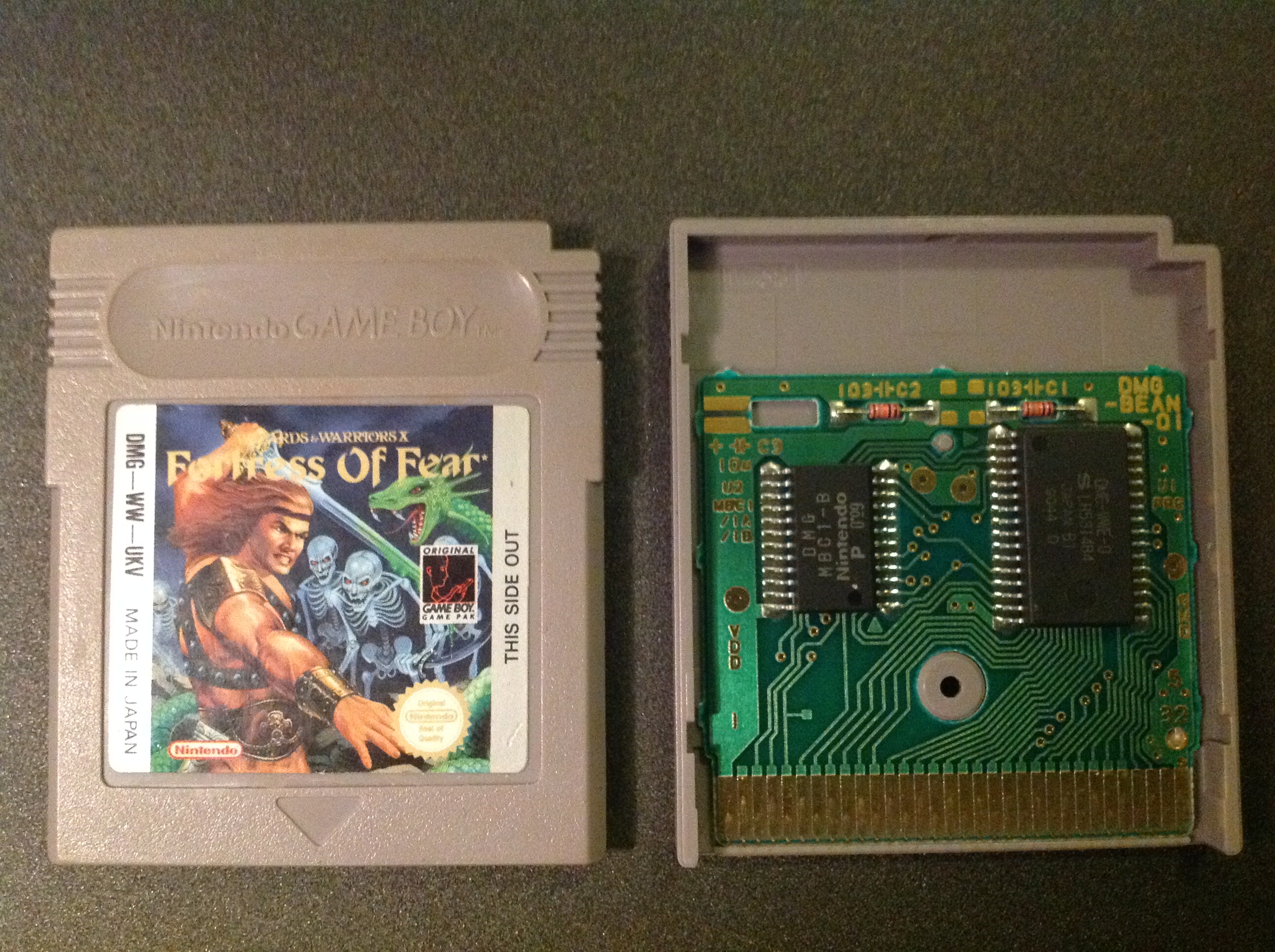
My cartridge has the code DMG-WW-UKV, which is probably the UK release of the game (?). The ROM dump matches with "Wizards & Warriors Chapter X - The Fortress of Fear (E) [!].gb" in the GoodGBX database, and the database doesn't have any other versions, so both European and American releases might have the same ROM. The ROM size is 512 Kbit (= 64 KB), which corresponds to a 16-bit address space ($0000 - $FFFF).
Cartridge PCB (printed circuit board)
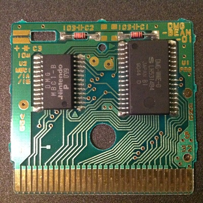
The PCB is DMG-BEAN-01, which is a very common board used in a lot of MBC1 games. MBC1 was the most common chip in original Gameboy games, so most RAMless MBC1 games have a similar layout. Unlike in the previous analysis, this time we can actually see the ROM chip on the right side of the board. A Gameboy ROM chip usually has a game- and version-specific code and a manufacturer part code, which in this case are DMG-WWE-0 and LH5314B4. On the left side we can see the MBC chip, which is labeled "MBC1-B".
Connections on the PCB
This time we can see all the connections, so things are a bit more interesting. Only CLK and VIN are not connected, although MREQ, WR and RS are in practice unused because no RAM chip is present. The address lines A0-A12 are only connected to the ROM chip, so the MBC doesn't care about those address bits. A13 is connected to both the MBC and the ROM, A14 is connected only to the MBC. A15 is connected to both, but it has a special purpose as outlined in the previous blog post.
In order to understand the purposes of the ROM pins, we need a data sheet for the ROM, but custom ROMs like this don't have public data sheets. However, it seems that the same pin layout can be found in similar off-the-shelf components from the same manufacturer. In this case, the same layout can be found in DIP/SOP-packaged Sharp LH531V00 even though it is a 1 MBit chip. So, we expect the layout to have 20 address pins, where one is unused in the 512 KBit ROM chip.
Update = Actually, many chips seem to follow the JEDEC 21-C standard, which defines a standard pin layout for ROM chips up to 8Mbit.
Based on the data sheet we can see that A0-A13 are directly connected to the corresponding pins in the ROM. Address pins 14-15 are connected to the MBC, so the MBC controls the upper 2 bits of the address the ROM chip sees. In the visualization I'm using the M14-M18 naming as used by Jeff Frohwein in his MBC1 schematics. M16, M17 and M18 are connected to the ROM chip, but the data sheet confirms they are unused. So, as a summary, the ROM address is composed of A0-A13 and M14-M15 giving us the full 16-bit address space as expected.
The data pins D0-D4 in the cartridge header are connected to both the MBC and the ROM. The remaining pins D5-D7 are connected only to the ROM. In practice this means that the MBC can only handle 5-bit values, while the ROM works with the full 8 bits.
The ROM data sheet also mentions the OE (= Output Enable) and CE (Chip Enable) pins. The OE pin is connected to the RD pin in the cartridge, and the CE pin is connected to the A15 pin in the cartridge. So, in order to read from the ROM, we need to have RD low and A15 low, so in practice the ROM chip will respond to reads in the $0000 - $7FFF address range, which is exactly as expected.
There's also 4 unused pins in the MBC chip, but I'll analyze them in a later blog post once we get to more complex cartridges where they are actually used.
Notes for emulators
Based on the connections in the PCB, we can summarize the following findings:
- Reading $0000 - $7FFF activates the ROM chip, but the physical ROM address is a combination of 14 bits from the address and 2 bits from the MBC
- MBC1 can access only address bits 13-15
- MBC1 can access only data bits 0-5
- MBC1 can access the WR, MREQ, and RS pins (this will be important later)
This is not yet enough information to emulate MBC1, but we'll get there after we analyze a couple more cartridges with the chip. In a later blog post I'll also show how MBC1 behaves when we peek and poke some addresses, and we'll find out what what bits the M14-M18 pins have in practice.